
Designing the PCB
Probably this will take up most of your time.
Keyboard Parts
Before you start placing components in KiCAD, it helps to know what everything actually is and how it fits together physically.
Switches
Switches are the mechanical components under each key, the part you actually press. When you press a key, the switch closes an electrical circuit that the Pico detects.
There are three main types:
- Linear: smooth and consistent from top to bottom, no bump or click. Popular for gaming.
- Tactile: a subtle bump partway through the press gives you feedback that the key registered. Quiet but noticeable.
- Clicky: has both a tactile bump and an audible click. Satisfying, but loud.
This project uses MX-style switches, which is the most common standard. Almost all aftermarket switches, keycaps, and plates are compatible with it.
Keycaps
Keycaps are the plastic caps that sit on top of each switch, the part your fingers touch. They pull off and snap back on, so they’re easy to swap.
Keycaps come in many profiles (the shape and height), but for this project DSA keycaps are a good choice because every key is the same height, which means one set fits any layout without worrying about rows.
Stabilizers
Wider keys (2u and above, like spacebar, backspace, left shift, and enter) would wobble if held only by their switch. Stabilizers are mechanical brackets that clip onto the PCB and keep both ends of the key moving evenly.
You only need stabilizers for keys that are 2u or wider. Anything smaller uses just the switch.
The Raspberry Pi Pico
The Pico is the microcontroller, the “brain” of the keyboard. It reads the switch matrix, figures out which key was pressed, and sends that keypress to your computer over USB.
The Pico solders directly onto your PCB through-hole. Its USB-C port will hang off the edge of the board slightly so you can plug a cable in.
It has 29 GPIO pins, which is why we use a matrix. A 60% keyboard has far more keys than available pins.
Diodes (1N4148)
Each switch has a 1N4148 diode wired in series with it. Diodes only let current flow one way, which prevents “ghosting”, a problem where pressing multiple keys at once confuses the matrix and registers phantom keypresses.
These are through-hole components (legs go through the PCB) and are straightforward to solder.
Optional Add-ons
If you want to go further, these parts can be added to your PCB:
| Part | What it does |
|---|---|
| RGB LEDs (SK6812 MINI-E) | Individually addressable color lighting under each key |
| Rotary encoder (EC11) | A dial you can turn, useful for volume, scrolling, etc. |
| OLED screen | A small display showing things like current layer or a logo |
| Buzzer | Audio feedback on keypresses |
These are all optional. You can keep it simple and just build a clean typing keyboard.
Setting Up KiCAD
Download and install the latest version of KiCAD from kicad.org.
Installing marbastlib
marbastlib is a KiCAD library with pre-made symbols and footprints for keyboard components. Without it, you won’t have access to the switch, stabilizer, or LED parts you need.
- Open KiCAD and go to Plugin and Content Manager in the main window.
- Click Manage next to Repositories, then hit the + button.
- Paste this URL into the field:
https://raw.githubusercontent.com/ebastler/ebastler-KiCad-repository/main/repository.json

- Switch to the ebastler KiCAD Repository tab, find the marbastlib library, and click Install.
- Click Apply Pending Changes, then close and fully reopen KiCAD for the libraries to load.
Creating a New Project
- In the KiCAD main window, go to File → New Project.
- Choose a folder and give your project a name (e.g.
my-keeb). - KiCAD creates two main files: a
.kicad_sch(schematic) and a.kicad_pcb(board layout). You’ll work in both.
Designing Your Schematic
The schematic is where you define all the electrical connections. Think of it as the wiring diagram before you worry about physical placement.
Opening the Schematic Editor
From the KiCAD project window, click the Schematic Editor button (the icon that looks like a circuit diagram), or double-click your .kicad_sch file.
Adding Symbols (Bringing In Parts)
- Press A (or go to Place → Add Symbol) to open the symbol chooser.
- In the search bar, type the part you want:
RaspberryPi_Picofor the Pico microcontrollerSW_Pushfor a key switchMX_stabfor a stabilizer (from marbastlib)1N4148for a diode
- Select the symbol and click OK. It will attach to your cursor. Click to place it on the schematic.
- Press Escape when you’re done placing.

Understanding the Keyboard Matrix
A full 60% keyboard has around 61 keys, but the Pico only has 29 GPIO pins, which is not enough for one wire per switch. The solution is a keyboard matrix.
In a matrix, switches are arranged in rows and columns. You only need one pin per row and one pin per column. A 6-row × 11-column matrix can handle 66 keys using just 17 pins.
To make the matrix work correctly, each switch needs a diode wired in series with it. Without diodes, pressing multiple keys at once causes “ghosting”, phantom keypresses that shouldn’t be there.
For a deeper explanation of how matrices work, see this guide.
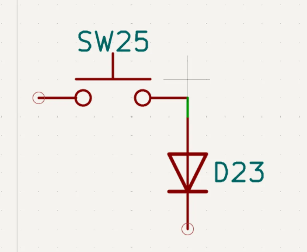
Wiring a Switch-Diode Unit
Each key is a pair: one switch and one diode. Wire them like this:
- Place a
SW_Pushsymbol and a1N4148diode next to each other. - Connect one leg of the diode to one pin of the switch using the Wire tool (press W).
- The other leg of the diode connects to the row line. The other switch pin connects to the column line.
Replicating Your Layout
Replicate the switch-diode unit for every key in your layout. Arrange them to match the physical layout of your keyboard from your sketch, with rows going left to right and columns going top to bottom.


Using Net Labels
Instead of drawing a wire all the way from each row/column to the Pico (which would make the schematic unreadable), use Net Labels:
- Press L (or go to Place → Net Label) to add a label.
- Name your rows
ROW0,ROW1,ROW2, etc. and your columnsCOL0,COL1, etc. - Attach matching labels to the corresponding pins on the Pico.
KiCAD treats any two wires with the same label as electrically connected, even if they aren’t physically drawn touching. The small green dots you see are junctions that confirm two wires are connected. If wires cross without a dot, they are not connected.

Adding Stabilizers
Stabilizers need to be placed in the schematic too so they get footprints on the PCB.
Only add a stabilizer for each key that is 2u or wider (spacebar, backspace, left shift, enter). For a standard 60% layout, that’s usually 3-4 stabilizers.
- Press A and search for
MX_stab. - Place one for each wide key in your layout.

Adding Mounting Holes
If you’re building a tray-mount case, add mounting holes to your schematic so they appear on the PCB.
- Press A and search for
MountingHole. - Place 4–6 holes around the edges and corners of where your board will be.
There are several mount styles, and each one changes the typing feel of the finished keyboard:

Annotating Your Schematic
Before you can move to the PCB layout, every component needs a unique reference designator (like SW1, D1, U1). This is called annotation.
- Go to Tools → Annotate Schematic.
- Leave the default settings and click Annotate.
KiCAD will automatically number all your components.


Assigning Footprints
A footprint tells KiCAD the physical size and pad layout for each component on the PCB. Every symbol in your schematic needs one.
- Go to Tools → Assign Footprints (or click the footprint icon in the toolbar).

- The left panel lists your component types. The right panel shows available footprints. The center panel shows your components.
Assigning the Pico
- Click
RaspberryPi_Picoin the left panel. - In the search bar on the right, type
RaspberryPi_Pico_Common_THT. - Double-click the result to assign it.
Assigning Diodes
- Click
D_1N4148(or whatever your diode symbol is named) in the left panel. - Hold Ctrl and click every diode in the center panel to select them all at once.
- Search for
Diode_THT:D_DO-35_SOD27_P7.62mm_Horizontalon the right. - Double-click to assign it to all selected diodes at once.
Assigning Switches
- Select all switch symbols (
SW_Push) in the center panel. - Search for
PCM_marbastlib-mx:SW_MX_1uon the right. - Double-click to assign.
Assigning Stabilizers
- Select all stabilizer symbols in the center panel.
- Search for
PCM_marbastlib-mx:STAB_MXon the right. - Double-click to assign.
Click OK when all footprints are assigned.
Designing Your PCB Layout
Now you move from the logical schematic to the physical board. Go back to the KiCAD project window and open the PCB Editor.
Importing from the Schematic
- In the PCB Editor, go to Tools → Update PCB from Schematic (or press F8).
- Click Update PCB. All your components will appear as a pile in the center of the screen.
It will look messy at first. That’s normal.

Setting Up the Board Outline
Before placing components, draw the outer edge of your PCB on the Edge.Cuts layer.
- In the right panel, select the
Edge.Cutslayer. - Use the Draw Rectangle tool (or Draw Line for custom shapes) to draw the outline of your board.
- A standard 60% keyboard is roughly 285mm × 95mm, but size it to fit your layout.
Placing Components
Start by placing the Pico, then build out from there.
- Click and drag components into position. Use R to rotate.
- Place the Pico at one edge of the board so its USB-C port hangs slightly off the PCB. This makes it easier to plug in a cable.
- Place switches according to your layout. Use a consistent spacing. MX switches use a 19.05mm grid.
- Place stabilizers directly under their corresponding wide keys.
- Place diodes near their switches, typically just below or above each one.
You can use whatever spacing works for you, just keep it consistent.

Geographical Reannotation
If you copy-pasted footprints, their reference numbers may be out of order. Use Geographical Reannotate to renumber them by their physical position on the board:
- Go to Tools → Geographical Reannotate.
- Choose your preferred order (left-to-right, top-to-bottom).
- Click OK. The references update to match position, and KiCAD will sync this back to your schematic.

Your PCB should look something like this after everything is laid out:

Routing Traces
Routing is the process of drawing the copper traces (wires) that connect all the pads together. The thin “ratsnest” lines show you which pads still need to be connected.
- Press X to activate the Route Track tool.
- Click a pad to start a trace, then click the destination pad to complete the connection.
- Use the
F.Culayer (front copper) for traces going in one direction andB.Cu(back copper) for the other direction. This keeps things organized and avoids most crossings. - Press / to switch between front and back copper mid-trace (this adds a via, a small hole that connects the two layers).
Tips:
- Route the Pico connections first since they touch everything.
- Keep traces as short and direct as possible.
- Avoid sharp 90-degree corners. Use 45-degree angles instead.


The USB port of the Pico should hang off the PCB edge slightly so a cable can plug in:

Adding a Ground Fill (Optional)
A ground fill floods any empty copper area on the board with a solid GND connection. It’s optional but good practice.
- Select the
F.Culayer. - Go to Place → Add Rule Area or use the Add Filled Zone tool.
- Draw a rectangle covering your entire board outline.
- In the dialog, set the net to
GNDand click OK. - Press B to fill all zones.
- Repeat on
B.Cu.
The finished board should look something like this:

Adding 3D Models
You can attach 3D models to footprints to visualize what your board will look like. Many footprints already include a model. For others (like the Pico), download a STEP file from GrabCAD and link it in the footprint properties.
To view your board in 3D, press Alt+3 or go to View → 3D Viewer.

Running the Design Rule Check
Before exporting, run a DRC to catch any mistakes:
- Go to Inspect → Design Rules Checker.
- Click Run DRC.
- Review any errors. Common ones are unconnected pads (ratsnest lines you missed) or traces that are too close together.
- Fix all errors before exporting.
Exporting Gerber Files
Now that the PCB is finished, it’s time to get it fabricated. Gerber files are the production files you send to a PCB manufacturer. Save your PCB, then go to File → Fabrication Outputs → Gerbers (.gbr) and export everything in that dialog.
If you want a known-good starting point, here are the exact settings to use.
Include these layers:
F.Cu, B.Cu, F.Paste, B.Paste, F.Silkscreen, B.Silkscreen, F.Mask, B.Mask, Edge.Cuts
General options:
| Option | Setting |
|---|---|
| Plot drawing sheet | off |
| Subtract soldermask from silkscreen | off |
| Indicate DNP on fabrication layers | on, set to Cross-out |
| Sketch pads on fabrication layers | off |
| Check zone fills before plotting | on |
| Drill marks | None |
| Scaling | 1:1 |
| Plot mode | Filled |
Gerber options:
| Option | Setting |
|---|---|
| Use Protel filename extensions | off |
| Generate Gerber job file | on |
| Use extended X2 format (recommended) | on |
| Include netlist attributes | on |
| Disable aperture macros | off |
| Coordinate format | 4.6, unit mm |
Once your settings match, click Plot to generate the Gerbers. Then click Generate Drill Files and click Generate Drill File to export the .drl file.
Finally, zip the entire output folder. That zip is what you send to the manufacturer, and you should commit it to your repo alongside your bom.csv and KiCad project files.
Next Steps
Now that your PCB is designed, move on to Designing the Case.